| Sallen-Key Second Order
Filter
|
||||||||||||||||||||||||||||||||||||
|
by Peter Foote
[ OT Articles | Intro BDS | BaffleStep | BaffleStep Compensation | PLLXO | Sallen-Key | XO Design | DiAural ] |
||||||||||||||||||||||||||||||||||||
| The Sallen-Key filter is a popular
filter due to it's versatility and ease of design. In this document I hope to outline
the design of the filter to give an understanding of the math behind the filter design
so that one can understand and build this type of filter. This document goes along
with two others that give the equations for some other types of filters (but no design
work). To begin the explanation I will use this diagram; |
||||||||||||||||||||||||||||||||||||
|
|
||||||||||||||||||||||||||||||||||||
|
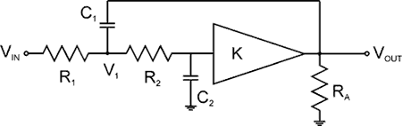
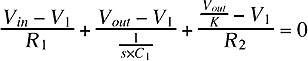
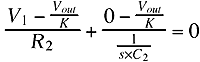
The K triangle represents a non-inverting amplifier. This means it takes the signal at the input (left), amplifies it by K, and outputs it (right). To get the initial equations to do the analysis just sum the current into a node (connection point). The currents must add up to zero. This has to be done for each node that isn't an input or output. For example, all the current flowing to the node marked V1 (through R1, C1, and R2) must add up to zero. Before creating the equations there are a few things to cover;
The value of s is used to indicate the frequency and phase of the capacitive reactance at the present frequency (not the cut-off frequency). |
||||||||||||||||||||||||||||||||||||
|
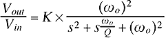
The standard second order filter equation is as follows;
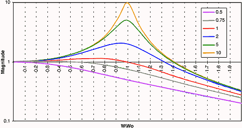
Where wo is the cut-off frequency of the filter (2 x pi x fo) and Q is the a factor that determines the shape of the filter curve. Sometimes the damping factor is mentioned in place of the Q, and it is just the inverse of Q. If you examine equation 3, you will see that at low frequencies the equation approaches K since the s terms are really small and don't have much affect. At high frequencies the equation approaches 0 since the s term becomes dominantly large. To give a better understanding of the relationship between Q and wo the following chart is provided. It shows that the magnitude of the response is equal to Q at wo. Varying the Q can be a useful tool to correct the response of a driver. Since this is for a low pass filter, you can see that the response begins at 1 for low frequecies and then tapers off at higher frequencies. The magnitude of the response at the cut-off frequency is dependant on the Q of the circuit.
Figure 1: Magnitude vs Normalized Frequency for Varying Values of Q Now that is out of the way, the equations to solve the filter are as follows;
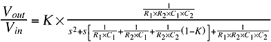
The above system equations (1 & 2) need to be solved so that V1 is eliminated and then the answer needs to be put into a form similar to equation 3. Solving equation 2 for V1 and then substituting into Equation 1 would be a good start. I won't show the math but rather just give the final answer. If you are so inclined then go ahead and do the math. The equation for the Sallen-Key low pass filter is as follows;
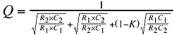
As you can see it becomes very complicated, quickly. To figure out the cut-off frequency and the Q of the filter, just match up the terms. This means the last term in the denominator is the cut-off frequency squared, or;
The middle term divided by the cut-off frequency and inverted is the Q, or;
Looking at these equations shows that there are 5 values that can be varied which can give the designer a lot of freedom. However, the varying of five separate elements isn't really necessary to allow the full use of this filter so some simplifications can be made.
Equal R, Unity Gain Case The most common way that this circuit is simplified is to make R1 = R2 = R and the gain equal to unity (K = 1). This simplifies the equations to;
Examining equation 7 shows us that the cut-off frequency is inversely proportional to R so the cut-off frequency can be adjusted, without affecting the Q, by varying the two resistors, while keeping them equal, using a dual ganged pot. The potentiometers should be put in series with a fixed resistor so that a range of frequencies can be selected. Examining equation 8 shows us that the Q of the filter is dependent only on the ratio of C1 to C2. To vary the Q of this filter, this ratio would have to be variable. If this ratio is variable, the cut-off frequency would vary as the Q was varied. Also, the filter would need a variable capacitor which usually isn't practical for this type of circuit. Therefore, using the equal R and K = 1 simplifications leaves us with a filter where the Q can't, practically, be made adjustable. One obvious problem to note is the capacitor selection. One capacitor can just be picked as a practical standard value but then the second one is fixed by the desired Q and it probably will not work out to be a standard value. This will then require some hand matching of different sized capacitors to get the right value. The way to do this would be to measure the first capacitor that is chosen, then calculate the value for the second capacitor, and then add together different capacitors to achieve this value (assuming it is a practical number). This will eliminate having to hand match both capacitors to design values.
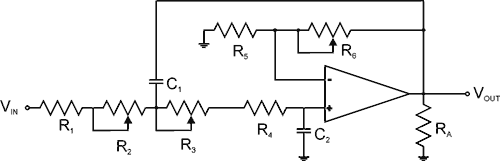
Example Now that the design equations are known, it is time to look at a practical example. For this example I will design a low pass filter with a variable crossover frequency and a Q of 0.707 (1/Q = damping d = square root of 2 or critically damped which is often considered the ideal). The drawing for the filter is as follows;
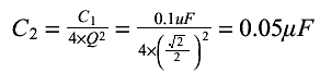
This filter has been refined by adding an op-amp, where the amplifier was, which is wired for unity gain. It also includes the variable resistors R2 and R3 that would be a dual ganged pot so that they remain equal at all times. To begin designing with this filter, I would chose the capacitor values. I'd set C1 as a 0.1 mF capacitor (why? its an available value so why not). To calculate C2, I rearrange equation 8 to solve for C2;
A 0.1 mF cap is easy to find and two 0.1mF caps in series would create the 0.05mF cap so these values are quite realistic. The only thing that would require a change would be unpractical resistance values. As a rule of thumb, I would consider any resistance between 10 kW and 200 kW as acceptable. Below this you could overload the op-amp output and above this you will reach a point where the circuit may become noisy. Now for the frequency. I think a variable frequency from 60 Hz to 120 Hz would be a good first design so I'll calculate the resistance values to see what they are. I rearrange equation 7 to solve for R;
This shows me that resistors R1 and R4 should be around 37 kW (standard value is 39 kW which is very close) to set the high frequency limit. The potentiometer for R2 and R3 would then have to be the difference between these resistance's which is 38 kW. Since this is a nonstandard value I would chose a 50 kW pot. You can calculate the new frequencies with these values but basically they will shift the low frequency cut-off point down about 10 Hz.
Equal R, Equal C Case The other common choice to make for this filter is R1 = R2 = R and C1 = C2 = C. The gain is left adjustable. The equations simplify to;
Examining Equation 9 shows us that the cut-off frequency of the filter is still selected by varying the resistor values using a dual ganged pot like the previous case. Examining Equation 10 shows us that the Q of the filter is dependent only on the gain of the amplifier. This is interesting because a filter can easily be made with an independently adjustable cut-off frequency and Q using this approach (as opposed to the previous approach). The disadvantage being that the gain of the circuit will change as the Q is adjusted.
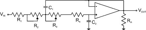
Example The practical version of this filter will look like the following;
This filter has been refined by adding an op-amp, where the amplifier was, that is wired to be non-inverting with variable gain. The other part of the circuit is the same as the previous example. For this circuit;
The values for these resistors and capacitors will be picked by using this equation, which is derived from Equation 9;
To solve this, pick a value for the capacitor and then calculate the resistance. The variable and fixed resistance's can be calculated in the same manner as they were for the previous example. To create the variable Q part of the circuit, the gain of the non-inverting op-amp must first be known. It is as follows;
Examining this equation shows us that when R6 = 0 that the gain of the op-amp will be 1 and that when R6 is at it's maximum the gain of the op-amp will also be its maximum. Since the lowest gain available with this circuit is 1 (R6 = 0) then we just need to calculate the maximum gain desired. With the gain of 1 fixed as the lowest value this sets the lowest Q possible at 0.5, from equation 10. When examining Equation 10 it can be seen that the gain should never be allowed to be equal to or greater than 3 since this would make the Q of the circuit approach infinity which creates a stability problem. Solving Equation 10 for the gain gives us;
To solve the problem with the gain changing as the Q is adjusted there are two possibilities. Add another op-amp before or after the circuit that is built the same as the op-amp and R5/R6 combo that is already in the circuit with the variable resistor wired so that it is at it's minimum when R6 is at its maximum and vice versa. This will automatically adjust the gain as the Q is varied but it adds another op-amp stage. If it is added before the filter it can be used as the input buffer as well. The other solution is to just not worry about it. You will probably add an input buffer that gives a gain adjustment so just compensate for a Q adjustment with a change in the input gain. Since the frequency is calculated the same way as in the previous case, I am just going to run through the variable Q calculations. A maximum value of Q equal to 10 may be desired so the gain in this case would be;
To realize this circuit we would pick a standard variable resistor value and then calculate the fixed resistance that would go along with it. For simplicity, I will once again pick a 50 kW pot. The fixed resistor is calculated by rearranging Equation 11;
To finish, pick a standard value that would be greater than this. The only consequence of this would be that the Q would not reach 10 as desired but this is better then having a circuit where the gain could reach 3, which would cause stability problems.
Other Considerations
|
||||||||||||||||||||||||||||||||||||
|
The circuit should have an input buffer consisting of another op-amp. This is because some equipment may have a fairly high output impedance which would then be in series with the first resistor in the circuit and then it would not be equal to the second resistance like it should. |
||||||||||||||||||||||||||||||||||||
| Many times the circuit is being
driven by a fairly low level signal. This can lead to excessive noise being generated
in the filter. A solution to this would be to put a high quality op-amp at the input
which boosts the gain and then a voltage divider at the output to lower the gain
again. A circuit always exibits the least amount of noise if the most gain is done
as close to the source as possible. This is because the rest of the circuit will
operate at higher voltage levels so the noise is a much lower percentage of the signal. As an aside to the above, the circuit should not be allowed to have such a high signal level going through it that one of the op-amp outputs will clip. Generally, an op-amp operating at 15 volt supplies has about 13.5 volts of output swing in the positive and negative direction. |
||||||||||||||||||||||||||||||||||||
|
[ Back to T-Line Speaker Page | OT Articles ] [ BaffleStep | BaffleStep Compensation | PLLXO | Sallen-Key | XO Design | DiAural ]
|